EBL system marks leap in quantum technology

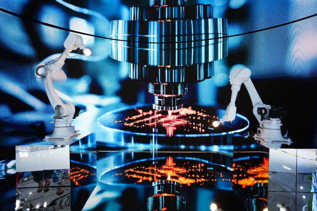
China's first commercial electron beam lithography system (EBL), "Xi Zhi", developed by Zhejiang University, has entered application testing, matching international precision standards and marking significant progress in domestic quantum chip research and development.
At the university's Yuhang institute for quantum innovation, the research team is rigorously testing the large, cabinet-like machine.
"This isn't an ordinary machine, but a 'nano-brush' capable of carving the map of an entire city on a single strand of hair!" the team leader said. Developed at a key provincial lab, the 100kV "Xi Zhi" system is now commercially available.
The system is named after Wang Xizhi, a famous Chinese calligrapher. "The difference is that it uses an electron beam instead of a brush, carving circuits on chips," a senior researcher said. Targeting quantum chips and advanced semiconductors, "Xi Zhi" directly "writes" circuits onto silicon wafers with 0.6 nanometer precision and 8 nanometer line width. It enables flexible design modifications without traditional photomasks. "In the early research and development phase, numerous design iterations requiring line-by-line adjustments are common. EBL offers high precision and convenience in 'writing,' greatly boosting efficiency in chip development," the researcher added.
The development of "Xi Zhi" breaks a critical barrier.
Previously, such cutting-edge technology was restricted by international export controls, leaving top institutions like the University of Science and Technology of China and Zhejiang University's own labs unable to procure it.
"Xi Zhi" is now in procurement discussions with entities like Huawei HiSilicon and multiple research institutes, priced below the international average.
The success of "Xi Zhi" stems from the "dual-new integration" model put forth by Zhejiang province, which merges technological and industrial innovation.
The application testing of "Xi Zhi" represents a major breakthrough in the localization of core high-end semiconductor equipment. This "graver", independently controlled by China, provides a solid foundation for accelerating the development of domestic high-end chips.
Yuhang district of Hangzhou is prioritizing integrated reforms in education, science, and talent, with AI as a key driver, to build a demonstration zone for innovation. Future efforts will focus on creating more landmark achievements through high-level platforms, talent, enterprises, projects, and tech finance.


